I cant believe THAT! said Alice.
Cant you? said the Queen in a pitying
tone.
Try again: draw a long breath, and
shut your eyes.
Alice laughed. Theres no use trying,
she
said, one cant believe impossible things.
I daresay you havent had much practice,
said the Queen. When I was your age, I
always did it for half-an-hour a day.
Why
sometimes I believed as many as six
impossible things before breakfast!
Through the Looking Glass (1871), Lewis Carroll
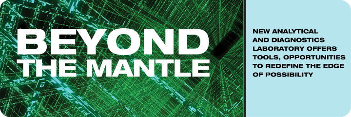
Impossible things arent quite what they used to be. But when Larry Lehman steps up to any of the looking glasses at his disposal, just like Alice, he is likely to soon find himself in an unfamiliar world comprising landscapes that defy experience, laws that flout established thinking and relationships that challenge convention.
Lehmans journeys beyond the mantle of the commonplace and past the edge of possibility are the result of science and technology rather than magic mirrors or psychotropic fungi. Still, in ways that neither Lewis Carroll nor the White Queen could ever have imagined, Lehmans efforts, and those of scores of other University and industry researchers who work alongside him, stand to underscore the advisability of believing the impossible.

Lehman is the manager of Binghamton Universitys Analytical and Diagnostics Laboratory (ADL). The facility, which is in the bioengineering building at the Innovative Technologies Complex, is the signature lab for Binghamtons Small Scale Systems Integration and Packaging Center (S3IP), a New York State Center of Excellence.
Arguably one of the best analytical facilities of its kind in the Northeast, the ADL is home to $16 million in state-of-the-art equipment, all in an 8,000-square-foot laboratory designed for functionality and flexibility. The facility was developed with state money to advance high-tech commercialization by making resources available for academic-industrial collaborations, said Mary Beth Curtin, associate director of the Center of Excellence. The facility will seek to become self-supporting through fees generated by users in the laboratory.
The multi-user facility opened its doors in September, and is expected to ramp up to full-scale operation during the next 18 to 24 months. By providing major instruments and technical support for diagnostics, analysis and characterization of materials used in small-scale systems integration and packaging, the laboratory will enable improvements to products and processes, which will translate into enhanced commercialization of microelectronics technologies, said Bahgat Sammakia, director of S3IP.
Technologies that will benefit from the ADL include electronics packaging, with products like computers and telecommunications, displays, new materials for electronics, organic electronics, defense and homeland security, and consumer products, Sammakia said. In other words, any technology that requires an understanding of materials behavior, molecular-level measurements and physics-based models of product performance in the field will benefit.
Binghamton University is already one of a handful of universities in the world that are at the forefront of research in electronic systems integration and packaging.
This lab will enable us to continue to compete and excel with this very distinguished and select group, Sammakia said.
The laboratory also builds on the Universitys successful track record of partnering with industry, particularly in the areas of electronics and micro- and flexible electronics. All under the S3IP umbrella, the ADL joins the Integrated Electronics Engineering Center and the Center for Advanced Microelectronics Manufacturing as another portal for companies seeking to take advantage of the extraordinary intellectual and physical research infrastructure the University provides.
Many small and even large multinational companies cannot justify investing in this infrastructure both instrumentation and scientists on their own, even though when they do need it, they will need it urgently, Sammakia said. The ADL enables regional and national industries to come to Binghamton and partner with us to conduct their R&D in key emerging technology fields.


As part of that kind of partnership, industries can tap not only into the physical infrastructure of the ADL, but also into the intellectual resources of more than 20 Binghamton faculty and scores of graduate students working in the area of small-scale systems integration and packaging. They can also count on support from PhD-level senior scientists and research engineers exclusively assigned to the laboratory.
One company that was quick to take advantage of the ADL is Corning Inc., where Ralph Truitt directs research in the area of characterization and materials processing.
Because of the breadth and ever-evolving types of technologies we support, and the capital-intensive nature of analytical measurements, we simply cant acquire every tool and expert we need, Truitt said. Partnering with labs that complement our capabilities is critical. The ADL at Binghamton University is just such a facility. The staffs expertise and the measurement tools that are being assembled are already a formidable set of capabilities to make unique surface chemistry analyses, material morphology measurements and thermal property measurements.
That will mean a savings in research time and expense and will allow Corning to leverage its expertise in developing new test applications, Truitt added.
We particularly appreciate the obvious attention paid to making access rules and administrative requirements clear and simple for consortium members, he said.
Samuel Chen, a senior research scientist with Eastman Kodak Co., agrees.
It was a real pleasant surprise to find a place like the ADL at Binghamton University with such a large number of high-tech analytical instruments capable of assisting the digital microelectronics effort of Eastman Kodak Co., Chen said. If we were to duplicate this type of analytical resource in Rochester, the cost would be prohibitively expensive. By being able to easily access ADL, this facility has provided us the complementary option to probe and understand different thin-film technologies needed for microelectronics and micromechanics.
Ultimately, the laboratory will put top-of-the-line tools in the hands of investigators, whether they are industry scientists, faculty researchers or graduate students, Lehman said.
If you want to see whats going on at the nanometer or micron level, these tools are just the best there is, he said. When it comes to microscopy, for instance, the ADL offers state-of-the-art solutions.
We go from extremely macro on one end a microscope that takes pictures at 0.3 magnification, so images are smaller than the actual thing, to equipment where we have several million magnification, Lehman said. Then we are looking at individual atom rows in material and can say, Well, in this particular layer here is where these two different crystals join together, and there is one layer of atoms there that is different. You can see it and you can measure it.
page 1 | page 2